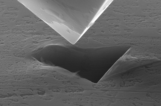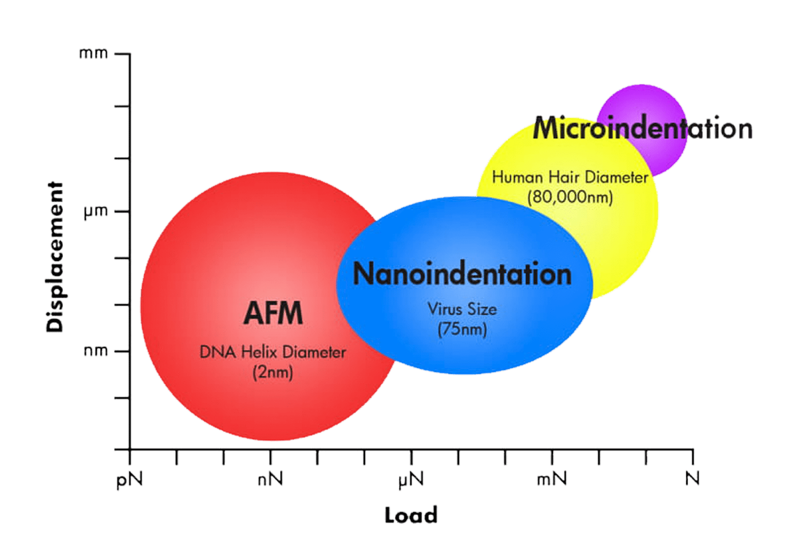
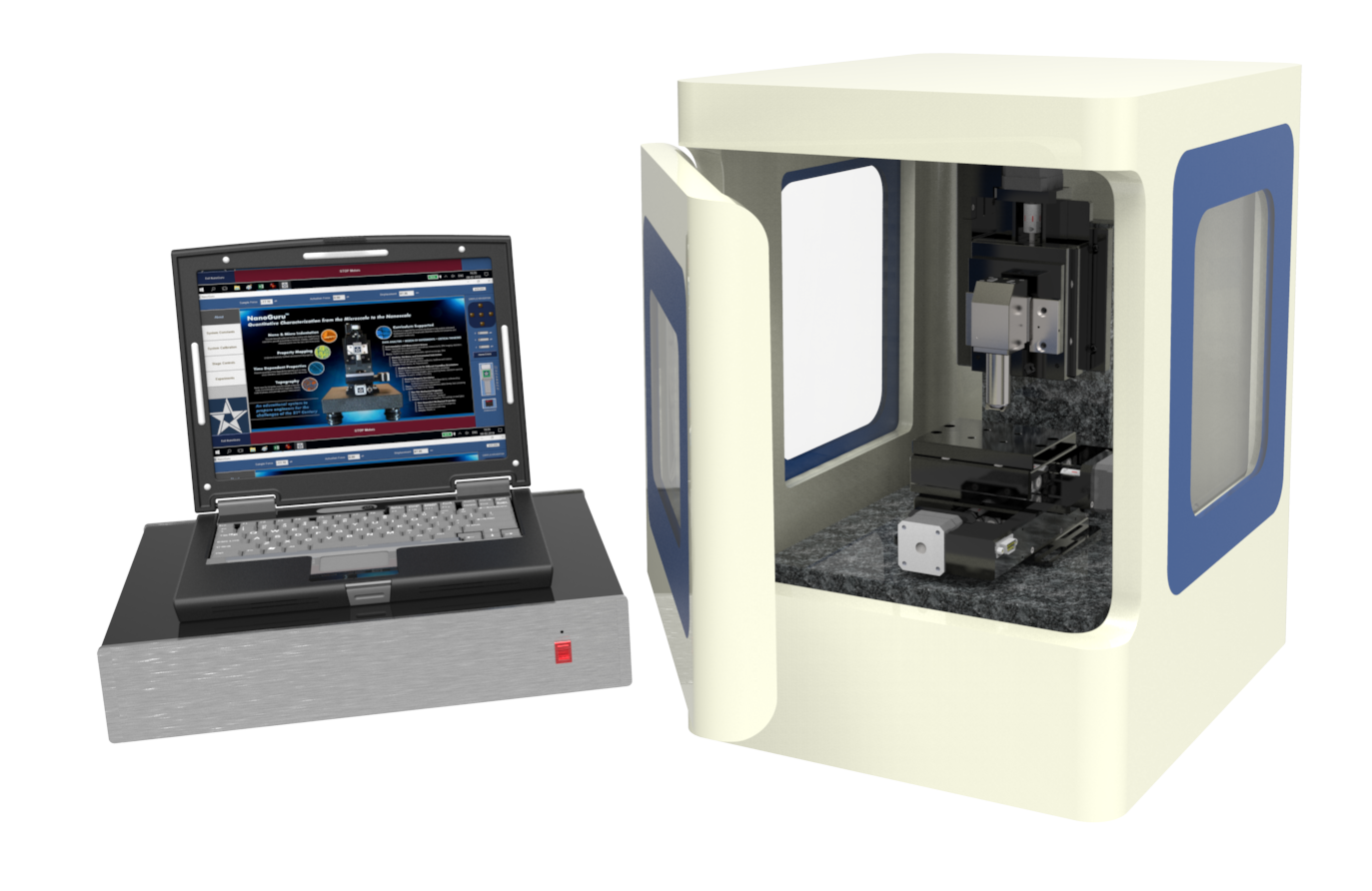
The NanoGuru is a scientific tool, designed and developed based on a technique called Nanoindentation, which helps the user to study mechanical properties of material at Nanoscale.
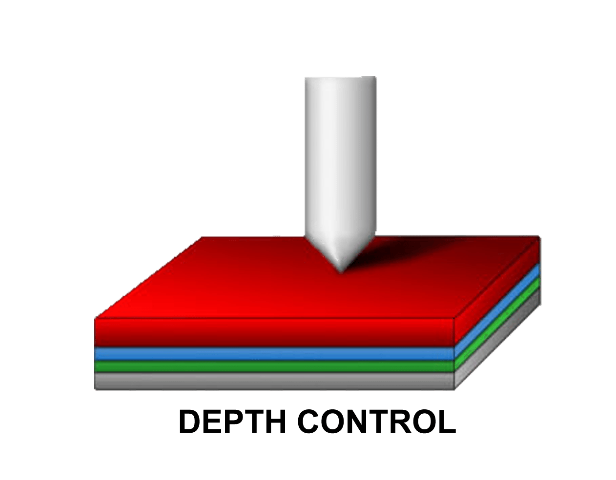
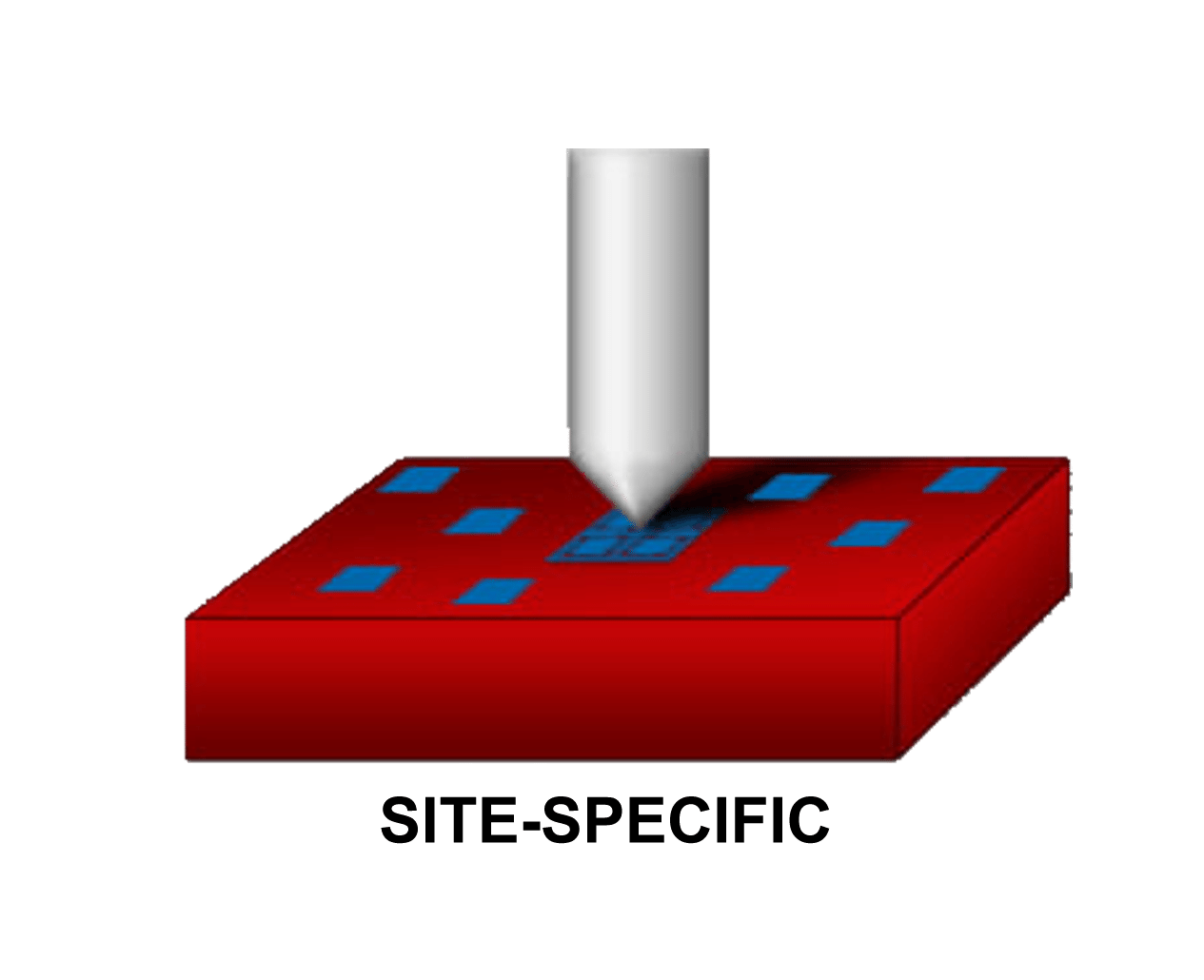
Properties can be measured at single or multiple locations as a function of indentation depth.
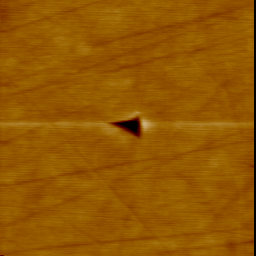
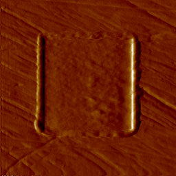
The NanoGuru incorporates In-situ Scanning Probe Microscopy (SPM) facility for high resolution 3D topographical mapping of the surface at nanoscale in real time for pre and post indent analysis.
Built-in vibration isolation for smaller foot print and portability with environmental enclosure to reduce noise.
24 bit DSP based controller for data acquisition and control.
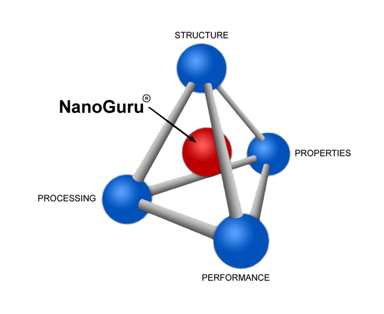
The NanoGuru offers the powerful Nanoindentation technique along with High resolution In-situ SPM facility to realize structure-property correlation of a given material at nanoscale.
The properties of a material are defined by its nanoscale structure.
The knowledge of nanoscale structure of a material defines its appropriate application.
The NanoGuru helps user to taps such nanoscale structural properties of a material to understand its behaviour to design better materials for the specific need.
Nanomechanical property measurement solutions from Industron.

No Need to be an expert, refer our practicum and start using it.

Footprint : 12"X12".
Weight : 32 kgs/70 lbs.

Set it up in 5 minutes and start your work.

Cost effective solution to your material characterization need at nanoscale
Strong specs, Impressive results.
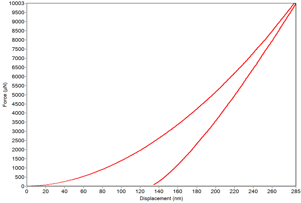
Force Noise Floor : < 150nN
Force Resolution: 1nN
Force Range : 10mN
Displacement Noise Floor : < 1nm
Displacement Resolution : < 0.006nm
Displacement Range : 5µm
SPM Image Size :50µm X 50µm
SPM Image Resolution :256 X 256
X, Y, Z Stage Travel : 50mm X 50mm X 50mm
XY Step Resolution : 50nm
Z Step Resolution : 10nm
Incredibly amazing results.
Tech support assistance providing solutions quickly.


All rights reserved ©2018 Industron Nanotechnology Pvt. Ltd.